PCB Manufacturing: From Design to Production
- 1 Understanding PCBs
- 2 The PCB Manufacturing Process
- 2.1 1. Design and Layout
- 2.2 2. Material Selection
- 2.3 3. Inner Layer Processing
- 2.4 4. Layer Alignment and Bonding
- 2.5 5. Drilling
- 2.6 6. Plating and Coating
- 2.7 7. Outer Layer Imaging
- 2.8 8. Solder Mask Application
- 2.9 9. Surface Finish
- 2.10 10. Silkscreen
- 2.11 11. Electrical Testing
- 2.12 12. Cutting and Profiling
- 2.13 13. Final Inspection and Packaging
- 3 Future Trends in PCB Manufacturing
- 3.1 3D Printing:
- 3.2 Flexible and Stretchable PCBs:
- 3.3 Embedded Components:
- 3.4 Smart Manufacturing:
- 3.5 Green Manufacturing:
- 4 Conclusion
The unsung hero of electronics is the Printed Circuit Boards (PCBs), without which our devices would not function. Being an integral part of most digital devices, PCBs form the crucial building blocks of today’s technology-laden society, from the mobile devices in our pockets to communication satellites orbiting our planet. In this blog post, I will explore the detailed process of producing PCBs, from designing to manufacturing them.
Understanding PCBs
So, before going deeper into the manufacturing process, let’s explain what a PCB is. A printed circuit board is an interconnecting device with electronic components joined by conductive paths, pads, and features. These components are produced by etching the insulated copper from sheets laminated on an insulating base. PCBs can be single-sided (One Copper Layer), double-sided (Two Copper Layers), or multi-layered.
The PCB Manufacturing Process
A complex series of actions must transform a circuit idea into a completed PCB. Let’s take a closer look at each of these.
1. Design and Layout
The most significant element of the creation of the PCB is the creation of the design. A chip engineer employs linear circuits Electronic Design Automation (EDA) software to develop a schematic view of the circuit. This is then translated to a printed circuit board layout where one defines the placement of the components and the interconnection paths.
Key considerations during the design phase include:
- Circuit functionality
- Component placement
- Signal integrity
- Power distribution
- Thermal management
- Manufacturing constraints
When the design is finished, it is exported as a collection of Gerber files, complete with all the data required for production.
2. Material Selection
Different materials used in the PCB production process determine its performance, lifespan, and cost. The primary material most often used is FR-4, an epoxy resin glass fiber reinforced laminate. Other materials such as polyimide, aluminum, and ceramics are also used for specific purposes.
Various factors impact the choice of material, such as:
- Operating temperature range
- Dielectric constant
- Thermal conductivity
- Coefficient of thermal expansion
- Cost
3. Inner Layer Processing
In the case of multi-layer PCB, the procedure starts from the internal layers of the respective PCB boards. The process typically involves these steps: The process typically involves these steps:
- Cleaning: The copper-clad laminate is first rinsed to wash away any contaminants from the surface.
- Photoresist Application: Coating of photoresist onto the copper layer This is a layer of photoresist applied onto the copper surface used in the etching process.
- Image Transfer: Typically, the circuit is formed when UV light transfers the circuit pattern onto the photoresist.
- Developing: This exposed and processed photoresist makes the circuit pattern whereby the unexposed portion of the photoresist is washed away.
- Etching: The rest of the copper is stripped off, thus exposing only the required copper traces.
- Stripping: They come through the top layer of resist, wash off the rest of the photoresist, and we can see the copper circuit pattern.
- Optical Inspection: Various inspections are done on the layers, including checking for defects.
4. Layer Alignment and Bonding
The separate layers of a multi-layer PCB must be aligned and glued together:
- Layer Up: The inner layers are placed with layers of prepreg placed between them; this material is a material that has been soaked in epoxy resin.
- Registration: They are accurately located in relation to each other through the use of the tooling holes.
- Bonding: In a lamination press, high pressure and temperature are applied, thus making the prepreg flow and laminating the stack.
5. Drilling
The PCB has various holes drilled for the component leads, which connect the different layers. This is usually achieved by using computerized drilling equipment for accuracy in terms of positions to be drilled. The types of holes include:
- Through-holes: Continue through all the layers
- Blind vias: Attach an outer shell to an inner compartment
- Buried vias: I: Integrate inner layers without going through the skin
6. Plating and Coating
The board goes through multiple plating and coating procedures after drilling.
- Desmear: This one clears any melted resin from the drilling process.
- Electroless Copper Deposition: A thin layer of copper is then dissolved by an electrolytic process on various parts of the board, even the holes.
- Copper Electroplating: A further increment of thickness is done by electroplating in copper.
- Tin Plating: This includes applying a thin layer of tin to cover the layer of copper so that it may be protected from etching.
7. Outer Layer Imaging
As with the outer layers, the photoresist is applied to the outer layers and then exposed and developed the same way that the inner layers are to form the circuit pattern through etching.
8. Solder Mask Application
Finally, a solder mask is provided to the board; this makes the PCB look green (but can also come in other colors). This layer:
- It avoids the formation of solder bridges between tiny and adjacent solder pads
- Acts as a shield to the copper traces against corrosion
- Provides electrical insulation
9. Surface Finish
Several surface finishes can be applied on exposed copper pads and traces to avoid oxidation and improve solderability. Common finishes include:
- Hot Air Solder Levelling (HASL)
- Electroless Nickel Immersion Gold [ENIG]
- Immersion Tin
- Immersion Silver
- Organic Solderability Preservative (OSP)
10. Silkscreen
All texts, signs, and symbols are applied with the help of silkscreen printing. This includes information on rightful designators of one or several components, distinctive threats or precautions, and the logos of their manufacturers.
11. Electrical Testing
Before the PCBs are shipped, they are subjected to an electrical test to check whether they have short circuits or open circuits.
- Flying Probe Test: Uses Moving probes to check connections.
- Bed of Nails Test: Goes to the test specification point and employs a fixture with spring-loaded pins that touch the test points.
12. Cutting and Profiling
In this case, it would be separated here if it had to produce one or more PCBs on a panel. One way to accomplish this is by:
- V-scoring and breaking
- Routing
- Laser cutting
13. Final Inspection and Packaging
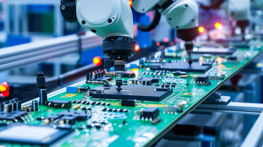
The manufactured PCBs are visually and optically inspected and tested using automated optical inspection. Automated Optical Inspection Aoi They are cleaned, packed, and ready for dispatch.
Future Trends in PCB Manufacturing
The PCB manufacturing sector is still developing. Among the new developments are:
-
3D Printing:
Currently, there are attempts to use AM technologies to make PCB prototypes and production designs.
-
Flexible and Stretchable PCBs:
There is a shift to developing new materials and manufacturing methods that would allow PCBs to flex or compress.
-
Embedded Components:
Components are now being placed directly into the PCB’s layers, offering an even higher density.
-
Smart Manufacturing:
Industry 4.0 concept is applied at the moment, and itted to manufacturing PCBs with data analysis and increased automation.
-
Green Manufacturing:
Sustainability has become an issue of concern within the clothing industry, where material use and waste production are also of concern.
Conclusion
Printed Circuit Board manufacturing is a complex process that involves lots of technology and finesse. Every stage of the creation process begins with careful planning and follows the exact sophisticated procedures to ensure the maximum quality. PCB manufacturing also remains ripe for further development in the years to come as technology continues to create more compact, faster, and more intricate electronics. Understanding this process not only makes the commoner appreciate the gadgets they use in their everyday life but also gives an insight into the upcoming electronics manufacturing processes.